Mackay School of Earth Science and Engineering
Microbeam Laboratory
University of Nevada, Reno
Descriptions of SEMs and their Capabilities
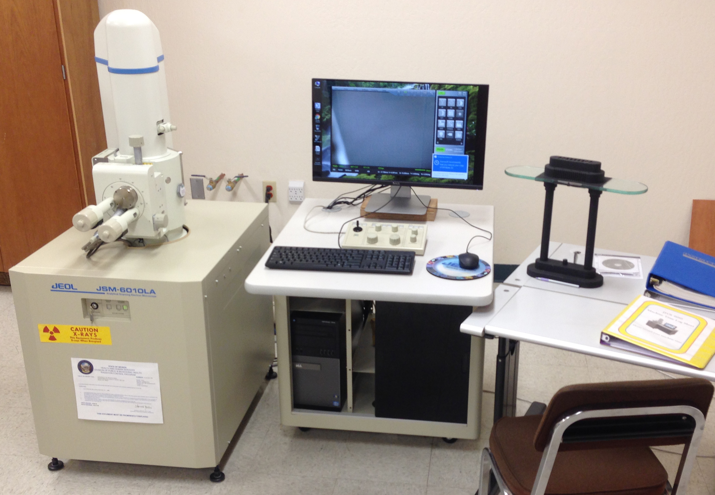
JEOL JSM-6010LA

The award-winning* JEOL JSM-6010LA is a compact, user-friendly, portable SEM with a tungsten filament source. It resolves down to less than 100 nm and its magnification ranges from 5- to 300,000X. The instrument includes an embedded energy dispersive X-ray spectrometer (EDS) for elemental analysis and mapping. The instrument can be operated in at both high and low vacuum, allowing for analysis of a wide variety of materials from geologic to biologic samples. A key differentiator of the 6010LA is the ease of use. Operation and control of the 6010LA is possible through a multi-touch screen interface, designed after touch-screen tablets, that allows users to undergo quick training and be independent users of the SEM in rapid time. Typical tasks such as automatic SEM condition setup and menus are based on sample types, including 1) metals/minerals, 2) biological samples, 3) organic specimens, 4) inorganic specimens, and 5) general purpose conditions. The ease of operation makes this SEM very accessible to a wide range of users.
*2011 R&D100 Award from R&D Magazine
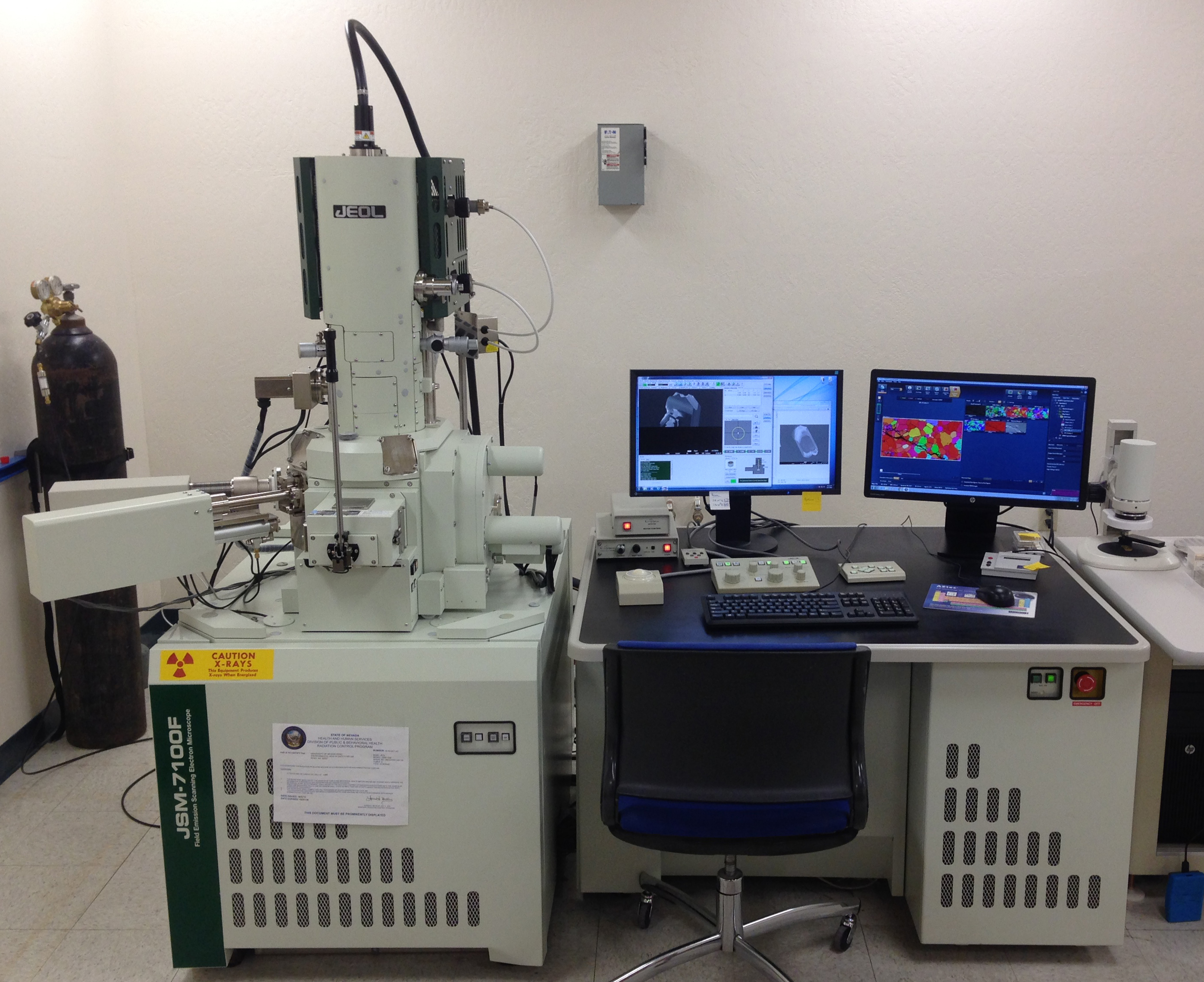
JSM-7100FT FESEM

The JSM-7100FT FESEM is a state of the art Schottky field emission SEM. It provides high resolution and very high and stable probe currents for optimum imaging and analytical performance at high vacuum. A combination of a large beam current with a small probe size at any accelerating voltage enables sub-nanometer spatial resolution and analytical characterization at the sub-100 nm scale. Magnification ranges from 25 to 1,000,000X. With the integration of the in-the-lens acceleration and deceleration of the electron beam, low kV aberrations are reduced, yielding high resolution at the lowest accelerating voltages. Beam deceleration decreases charging while imaging non-conductive specimens, improves spot size at low kV, and enhances surface topography. For example, nanometer-sized pores in shale can be imaged in beam deceleration mode. The 7100FT is equipped with several detectors including a Deben panchromatic cathodoluminescence (CL) detector, an Oxford Aztec EDS system with a 50 mm2 silicon drift detector, and an Oxford NordlysMax2 electron backscatter diffraction (EBSD) camera. The Oxford Aztec Microanalysis System includes all the hardware and software tools to perform chemical analysis, image capture, and X-ray spectral mapping and line scanning. For example, it has the ability to automatically search a polished thin section for electrum or native gold grains.
Applications to Earth and Material Sciences
Scanning electron microscopy provides an essential observational tool to investigate micron-scale characteristics of natural and fabricated samples. Combining backscatter electron (BSE), energy dispersive X-ray spectroscopy (EDS), cathodoluminescence (CL), and electron backscatter diffraction (EBSD) analyses with state of the art SEMs allows for the acquisition of qualitative chemical compositions through EDS, crystal growth and trace elements contained in minerals through CL, and crystalline structure and orientation through EBSD. High-resolution images reveal chemical variations by EDS elemental mapping or spot chemical analyses and by discriminating phases based on mean atomic number using BSE. Thus, SEM instruments provide a wealth of information in the study of solid materials with abundant geological, environmental and material science applications.
Secondary electron (SE) imaging
The JEOL 6010LA and 7100FT FESEM are both equipped with secondary electron (SE) detectors, whereas the 7100FT FESEM has the capabilities of resolving surface topography in three dimensions with a rotating stage that produces extremely high-resolution images. Scattering of secondary electrons emitted from just below the sample surface upon interaction with the electron beam provide a means of examining sample topography from the micron to nanometer scale. Thin sections or samples that are massive or powdered are typically coated with carbon or gold before direct observation with the SE detector. Direct applications for nanometer scale SE imaging are in the fields of sedimentary petrography (i.e., fine-grained clay particle morphology, porosity in oil-shales, quartz grain boundaries and individual grain morphology, soils), paleontology (fossil identification and classification), biology (cell studies), chemistry (polymer studies), and materials (electronic components).
Example applications: Industrial Minerals | Paleontology | Engineering and Material Sciences
Backscatter electron (BSE) imaging
The JEOL 6010LA and 7100 FESEM are both equipped with backscatter electron (BSE) detectors. Scattering of electrons, backscatter electrons, from beam–sample interaction causes collisions with atoms. The larger atoms with higher atomic number have a higher probability of causing collisions. The result in the number of backscatter electrons that reach the detector is proportional to the mean atomic number of the material being analyzed. As a result, the brighter materials in an image have higher mean atomic numbers than the darker materials. Thus, high-resolution BSE images can assist in phase composition, identification, and abundance, as well as textural relationships. Backscatter electron images are useful in sedimentary, igneous, and metamorphic petrology, the study of mineral deposits, metallurgy and materials science, among many other fields.
Example applications: Ore Deposits | Petrology and Tectonics
Energy dispersive X-ray spectroscopy (EDS)
The JEOL 6010LA and 7100FT FESEM are both equipped with energy dispersive X-ray spectrometers (EDS) that characterize X-rays generated from the incident electron beam into an energy spectrum that determines element abundances. The new generation X-MaxN large area detector on the 7100FT is capable of producing high-resolution maps with high speed and accuracy, whereas the 6010LA can fulfill all EDS spot analysis needs. The EDS detector measures the number and energy of X-rays emitted from a specimen, allowing for measurement of elemental composition. This powerful tool can determine the chemical composition down to a spot size of a few microns and can raster over a larger area to produce chemical composition maps. Geologic samples typically consist of fine-grained aggregates of minerals that are difficult to identify. EDS elemental mapping provides key information pertaining to the spatial distribution of elements, which can assist in observing heterogeneity at the micron scale. Direct applications of EDS analyses are extremely useful in ore, sedimentary, igneous, and metamorphic petrology (phase identification, mineral chemical zoning, replacement reactions), geochronology (inclusion identification), and soil science (mineral identification).
Example applications: Ore Deposits | Petrology and Tectonics | Orthoamphibole Gneiss
Cathodoluminescence (CL) imaging
The JEOL 7100FT FESEM is equipped with a cathodoluminescence (CL) detector that generates high-resolution digital CL images of minerals on the micron to nanometer scale. The beam–sample interaction for specific minerals (e.g., quartz, zircon) causes excitation of valence electrons, which emits photons that may have wavelengths in the visible spectrum. The CL emission provides general information on the trace elements or deformation within crystals. Moreover, CL emissions provide key information on crystal growth history (single grains and/or within veins), internal structure, and provenance. Applications in geology are dominantly related to in situ U-Pb, trace element, and stable isotope studies of accessory minerals (zircon, baddeleyite, xenotime, apatite) to determine timing of crystallization or metamorphism, compositions of magmas/fluids, and P–T conditions from which the minerals (re)crystallized. In addition, ore and sedimentary petrology also utilize high-resolution CL images to identify specific growth phases in veins or cements for further microanalysis including EDS, fluid inclusions, and stable isotopes.
Example applications: Epithermal gold-bearing quartz vein | Accessory Minerals
Electron backscatter diffraction (EBSD)
The JEOL 7100FT FESEM is equipped with an electron backscatter diffraction (EBSD) detector consisting of phosphor screen with forescatter diodes (FSD) and a sensitive camera to view kikuchi patterns related to crystal orientation. The diffraction of electrons by atomic layers results from the interaction of the beam with an inclined sample (~70º), and these electrons generate visible lines (the kikuchi patterns) that represent projections of the lattice planes in the crystal. These patterns are digitized and processed by software to identify the orientation of phases, including the seven crystal systems. In addition to orientation, the data can be used to measure grain size, textures, zones of recrystallization, strain, phase identification, distribution of phases, phase transformations, fractures, and slip systems. Single grains can be analyzed or a larger area of the sample can be mapped.
Careful preparation of thin sections and metal alloys for successful EBSD analysis is required due to the likely introduction of crystal damage in the uppermost surface during initial typical polishing steps. To remove the surface damaged zone, thin sections and metal alloys receive a final polish with our vibratory polisher (Buehler Vibromet 2) in order to yield excellent EBSD results. EBSD sample preparation is included in the rate for use of the JEOL 7100FT FESEM.
Example applications: Engineering and Material Sciences
The application of the SEMs and their detectors to various problems of natural and man-made materials is limited mainly by the ingenuity of the investigator!